Programmed I/O
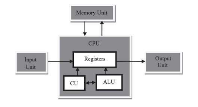
In the simplest method for performing I/O, an I/O module is connected to a pair of I/O registers in the CPU via a bus, with the I/O data register as the interface between the CPU and the buffer. Input from the peripheral device is transferred from the I/O module or buffer for that peripheral device one word at a time to the I/O data register and from there to an accumulator register under program control. Similarly, individual words of output data pass from an accumulator register to the I/O data register where they can be read by the appropriate I/O module, again under program control. Each instruction produces a single input or output. This method is known as programmed I/O.
In practice, it is most likely that there will be multiple devices connected to the CPU. Since each device must be recognized individually, address information must be sent with the I/O instruction. The address field of the I/O instruction can be used for this purpose. An I/O address register in the CPU holds the address for transfer to the bus. Each I/O module will have an identification address that will allow it to identify I/O instructions addressed to it and to ignore other I/O not intended for it.
Programmed I/O is obviously slow, since a full instruction fetch-execute cycle must be performed for each and every I/O data word to be transferred. Programmed I/O is used today primarily with keyboards, with occasional application to other simple character based data transfers, such as the transmission of commands through a network I/O module or modem. These operations are slow compared with the computer, with small quantities of data that can be handled one character at a time. One limitation, which we shall address is that with programmed I/O, input from the keyboard is accepted only under program control. An alternative means must be found to accept unexpected input from the keyboard.


Comments
Post a Comment