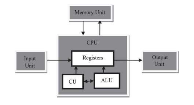
Von Neumann Architecture
- Four major subsystems called memory, input/output, the arithmetic/ logic unit (ALU), and the control unit. These four subsystems are diagrammed in Figure 5.2. The ALU and the control unit are often bundled together in what is called the Central Processing Unit or CPU.
- The stored program concept, in which the instructions to be executed by the computer are represented as binary values and stored in memory.
- The sequential execution of instructions, in which one instruction at a time is fetched from memory and passed to the control unit, where it is decoded and executed.

- Memory is divided into fixed-size units called cells, and each cell is associated with a unique identifier called an address. These addresses are the unsigned integers 0, 1, 2, ..., MAX.
- All accesses to memory are to a specified address, and we must always fetch or store a complete cell—that is, all the bits in that cell. The cell is the minimum unit of access.
- The time it takes to fetch or store the contents of a cell is the same for all the cells in memory.


Cache Memory.
When Von Neumann created his idealised model of a computer, he described only a single type of memory. Whenever the computer needed an instruction or a piece of data, Von Neumann simply assumed it would get it from RAM using the fetch operation just described. However, as computers became faster, designers noticed that, more and more, the processor was sitting idle waiting for data or instructions to arrive. Processors were executing instructions so quickly that memory access was becoming a bottleneck. (It is hard to believe that a memory unit that can fetch a piece of data in a few billionths of a second can slow anything down, but it does.) As the following graph shows, during the period from 1980 to 2000, processors increased in performance by a factor of about 3,000, whereas memories became faster by a factor of only about 10." This led to a huge imbalance between the capabilities of the processor and the capabilities of memory.

To solve this problem, designers needed to decrease memory access time to make it comparable with the time needed to carry out an instruction. It is possible to build extremely fast memory, but it is also quite expensive, and providing a few billion bytes or so of ultra-high-speed memory would make a computer prohibitively expensive.
However, computer designers discovered that it is not necessary to construct all of the memory from expensive, high-speed cells to obtain a significant increase in speed. They observed that when a program fetches a piece of data or an instruction, there is a high likelihood that
-
It will access that same instruction or piece of data in the very near future.
-
It will soon access the instructions or data that are located near that piece of data, where “near” means an address whose numerical value is close to this one.

When the computer needs a piece of information, it does not immediately do the memory fetch operation described earlier. Instead, it carries out the following three steps:
1. Look first in cache memory to see whether the information is there. If it is, then the computer can access it at the higher speed of the cache.
2.If the desired information is not in the cache, then access it from RAM at the slower speed, using the fetch operation described earlier.
3. Copy the data just fetched into the cache along with the k immediately following memory locations. If the cache is full, then discard some of the older items that have not recently been accessed. (The assumption is that we will not need them again for a while.)
This algorithm significantly reduces the average time to access information. For example, assume that the average access time of our RAM is 10 nsec, whereas the average access time of the cache is 2 nsec. Furthermore, assume that the information we need is in the cache 70% of the time, a value called the cache hit rate. In this situation, 70% of the time we get what we need in 2 nsec, and 30% of the time we have wasted that 2 nsec because the information is not in the cache and must be obtained from RAM, which will take 10 nsec. Our overall average access time will now be
which is a 50% reduction in access time from the original value of 10 nsec. A higher cache hit rate can lead to even greater savings.
A good analogy to cache memory is a home refrigerator. Without one we would have to go to the grocery store every time we needed an item; this corresponds to slow, regular memory access. Instead, when we go to the store we buy not only what we need now but also what we think we will need in the near future, and we put those items into our refrigerator. Now, when we need something, we first check the refrigerator. If it is there, we can get it at a much higher rate of speed. We only need to go to the store when the food item we want is not there.
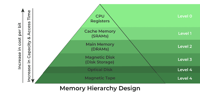
Caches are found on every modern computer system, and they are a significant contributor to the higher computational speeds achieved by new machines. Even though the formal Von Neumann model contained only a single memory unit, most computers built today have a multilevel hierarchy of random access memory.
Input/Output and Mass StorageThe input/output (I/0) units are the devices that allow a computer system to communicate and interact with the outside world as well as store information. The random access memory described in the previous section is volatile memory—the information disappears when the power is turned off. Without some type of long-term, nonvolatile memory, information could not be saved between shutdowns of the machine. Nonvolatile storage is the role of mass storage systems such as disks and tapes.
Of all the components of a Von Neumann machine, the I/O and mass storage subsystems are the most ad hoc and the most variable. Unlike the memory unit, I/O does not adhere to a single well-defined theoretical model. On the contrary, there are dozens of different I/O and mass storage devices manufactured by dozens of different companies and exhibiting many alternative organizations, making generalizations difficult. However, two important principles transcend the device-specific characteristics of particular vendors—I/O access methods and I/O controllers.
Input/output devices come in two basic types: those that represent information in human-readable form for human consumption and those that store information in machine-readable form for access by a computer system. The former includes such well-known I/O devices as keyboards, screens, and printers. The latter group of devices includes flash memory, hard drives, CDs, DVDs, and streaming tapes. Mass storage devices them- selves come in two distinct forms: direct access storage devices (DASDs) and sequential access storage devices (SASDs).
The fundamental characteristics of random access are:
1. Every memory cell has a unique address.
2. It takes the same amount of time to access every cell.
A direct access storage device is one in which requirement number 2, equal access time, has been eliminated. That is, in a direct access storage device, every unit of information still has a unique address, but the time needed to access that information depends on its physical location and the current state of the device.
The best examples of DASDs are the types of disks listed earlier: hard drives, CDs, DVDs, and so on. A disk stores information in units called sectors, each of which contains an address and a data block containing a fixed number of bytes.A fixed number of these sectors are placed in a concentric circle on the surface of the disk, called a track:


Finally, the surface of the disk contains many tracks, and there is a single read/write head that can be moved in or out to be positioned over any track on the disk surface. The entire disk rotates at high speed under the read/write head. The overall organization of a typical disk is shown in Figure 5.8.

The access time to any individual sector of the disk is made up of three components: seek time, latency, and transfer time. Seek time is the time needed to position the read/write head over the correct track; latency is the time for the beginning of the desired sector to rotate under the read/write head; and transfer time is the time for the entire sector to pass under the read/write head and have its contents read into or written from memory. These values depend on the specific sector being accessed and the current position of the read/write head. Let’s assume a disk drive with the following physical characteristics:
Rotation speed = 7,200 rev/min = 120 rev/sec = 8.33 msec/rev (1 msec = 0.001 sec)
Arm movement time = 0.02 msec to move to an adjacent track (i.e., moving from track j to either track i+1 or i— 1)
Number of tracks/surface = 1,000 (numbered 0 to 999)
Number of sectors/track = 64
Number of bytes/sector = 1,024
The access time for this disk can be determined as follows.
1. Seek Time
Best case = 0 msec (no arm movement)
Worst case = 999 x 0.02 = 19.98 msec (move from track 0 to track 999)
Average case = 300 x 0.02 = 6 msec (assume that on aver-age, the read/write head must move about 300 tracks)
2. Latency
Best case = 0 msec (sector is just about to come under the read/write head)
Worst case = 8.33 msec (we just missed the first bit of the sector and must wait one full revolution)
1/64 X 8.33 msec = 0.13 msec (the time for one sector, or 1/64th of a track, to pass under the read/write head; this time will be the same for al sectors)
The second type of mass storage device uses the old access technique called sequential access. A sequential access storage device (SASD) does not require that all units of data be identifiable via unique addresses. To find any given data item, we must search all data sequentially, repeatedly asking the question, “Is this what I'm looking for?” If not, we move on to the next unit of data and ask the question again. Eventually we find what we are looking for or come to the end of the data.
A sequential access storage device behaves just like the old audio cassette tapes of the 1980s and 1990s. To locate a specific song, we run the tape for a while and then stop and listen. This process is repeated until we find the desired song or come to the end of the tape. In contrast, a direct access storage device behaves like a CD or DVD that numbers al the songs and allows you to select any one. (The song number is the address.) Direct access storage devices are generally much faster at accessing individual pieces of information, and that is why they are much more widely used for mass storage. However, sequential access storage devices can be useful in specific situations, such as sequentially copying the entire contents of memory or of a disk drive. This backup operation fits the SASD model well, and streaming tape backup units are common storage devices on computer systems.
It is not uncommon for I/O operations such as displaying an image on a monitor or printing a page on a printer to be 3, 4, 5, or even 6 orders of magnitude slower than any other aspect of computer operation. If there isn’t something in the design of a computer to account for this difference, components that operate on totally incompatible time scales will be trying to talk to each other, which will produce enormous inefficiencies. The high- speed components will sit idle for long stretches of time while they wait for the slow I/O unit to accept or deliver the desired character. It would be like talking at the normal human rate of 240 words/min (4 words/sec) to someone who could respond only at the rate of 1 word every 8 hours—a difference of 5 orders of magnitude. You wouldn't get much useful work done!
The solution to this problem is to use a device called an I/O controller.
An I/O controller is like a special-purpose computer whose responsibility is
to handle the details of input/output and to compensate for any speed differences between I/O devices and other parts of the computer. It has a small
amount of memory, called an I/O buffer, and enough I/O control and logic
processing capability to handle the mechanical functions of the I/O device,
such as the read/write head, paper feed mechanism, and screen display. It
is also able to transmit to the processor a special hardware signal, called an
interrupt signal, when an I/O operation is done.
The organization of a typical I/O Controller is shown in Figure 5.9.
Let’s assume that we want to display one line (80 characters) of text
on a screen. First, the 80 characters are transferred from their current location in memory to the I/O buffer storage within the I/O controller. This
operation takes place at the high-speed data transfer rates of most computer
components—hundreds of millions of characters per second. Once this information is in the I/O buffer, the processor can instruct the I/O controller to
begin the output operation. The control logic of the I/O controller handles
the actual transfer and display of these 80 characters to the screen. This transfer may be at a much slower rate—perhaps only hundreds or thousands
of characters per second. However, the processor does not sit idle during this
output operation. It is free to do something else, perhaps work on another
program. The slowness of the I/O operation now affects only the I/O controller. When all 80 characters have been displayed, the I/O controller sends
an interrupt signal to the processor. The appearance of this special signal
indicates to the processor that the I/O operation is finished.

The arithmetic/logic unit (ALU) is the subsystem that performs such mathematical and logical operations as addition, subtraction, and comparison for equality. Although they can be conceptually viewed as separate components, in all modern machines the ALU and the control unit (discussed in the next section) have become fully integrated into a single component called the processor (the CPU). However, for reasons of clarity and convenience, we will describe the functions of the ALU and the control unit separately.
The ALU is made up of three parts: the registers, the interconnections between components, and the ALU circuitry. Together these components are called the data path.
A register is a storage cell that holds the operands of an arithmetic operation and that, when the operation is complete, holds its result. Registers are quite similar to the random access memory cells described in the previous section, with the following minor differences:
- They do not have a numeric memory address but are accessed by a special register designator such as A, X, or R0.
- They can be accessed much more quickly than regular memory cells. Because there are few registers (typically, a few dozen up to a hundred), it is reasonable to utilize the expensive circuitry needed to make the fetch and store operations 5 to 10 times faster than regular memory cells, of which there will be billions.
- They are not used for general-purpose storage but for specific purposes such as holding the operands for an upcoming arithmetic computation.
For example, an ALU might have three special registers called A, B, and C. Registers A and B hold the two input operands, and register C holds the result. This organization is diagrammed in Figure 5.10.

In most cases, however, three registers are not nearly enough to hold al the values that we might need. A typical ALU has 16, 32, or 64 registers. A more typical ALU organization is illustrated in Figure 5.11, which shows an ALU data path containing 16 registers designated R0 to R15. Any of the 16 ALU registers in Figure 5.11 could be used to hold the operands of the computation, and any register could be used to store the result.
To perform an arithmetic operation with the ALU of Figure 5.11, we first move the operands from memory to the ALU registers. Then we specify which register holds the left operand by connecting that register to the communication path called “Left.” In computer science terminology, a path for electrical signals (think of this as a wire) is termed a bus. We then specify which register to use for the right operand by connecting it to the bus labeled “Right.” (Like RAM, registers also use nondestructive fetch so that when it is needed, the value is only copied to the ALU. It is still in the register.) The ALU is enabled to perform the desired operation, and the answer is sent to any of the 16 registers along the bus labeled “Result.”


Machine Language Instructions. The instructions that can be decoded and executed by the control unit of a computer are represented in machine language. Instructions in this language are expressed in binary, and a typical format is shown in Figure 5.14.

The operation code field (referred to by the shorthand phrase op code) is a unique unsigned integer code assigned to each machine language operation recognized by the hardware. For example, 0 could be an ADD, 1 could be a COMPARE, and so on. If the operation code field contains k bits, then the maximum number of unique machine language operation codes is 2^k.
The address field(s) are the memory addresses of the values on which this operation will work. If our computer has a maximum of 2^N memory cells, then each address field must be N bits wide to enable us to address every cell because it takes N binary digits to represent al addresses in the range 0 to 2^N— 1. The number of address fields in an instruction is typically ranges from 0 to about 3, depending on what the operation is and how many operands it needs to do its work. For example, an instruction to add the contents of memory cell X to memory cell Y requires at least two addresses, X and Y. It could require three if the result were stored in a location different from either operand. In contrast, an instruction that tests the contents of memory cell X to see whether it is negative needs only a single address field, the location of cell X.
To see what this might produce in terms of machine language instructions, let's see what the following hypothetical instruction would actually look like when stored in memory:
ADD X, Y Add contents of memory addresses X and Y and put the sum back into memory address Y.
Let's assume that the op code for ADD is a decimal 9, X and Y correspond to memory addresses 99 and 100 (decimal), and the format of instructions is

A decimal 9, in 8-bit binary, is 00001001. Address 99, when converted to an unsigned 16-bit binary value, is 0000000001100011. Address 100 is : 0000000001100100. Putting these values together produces the instruction ADD X, Y as it would appear in memory:
00001001 0000000001100011 0000000001100100
This is somewhat cryptic to a person, but is easily understood by a control unit.
For clarity, we will not show these instructions in binary, as we did earlier. Instead, we will write out the operation code in English (for example, ADD, COMPARE, MOVE); use the capital letters X, Y, and Z to symbolically represent binary memory addresses; and use the letter R to represent an ALU register. Remember, however, that this notation is just for convenience. All machine language instructions are stored internally using binary representation.
The set of al operations that can be executed by a processor is called its instruction set, and the choice of exactly what operations to include or exclude from the instruction set is one of the most important and difficult decisions in the design of a new computer.
he machine language operations on most machines are quite elementary, and each operation typically performs a very simple task. The power of a processor comes not from the sophistication of the operations in its instruction set, but from the fact that it can execute each instruction very quickly, typically in a few billionths of a second.
One approach to designing instruction sets is to make them as small and as simple as possible, with perhaps as few as 30-50 instructions. Machines with this sort of instruction set are called reduced instruction set computers or RISC machines. This approach minimizes the amount of hardware circuitry (gates and transistors) needed to build a processor. The extra space on the chip can be used to optimize the speed of the instructions and allow them to execute very quickly. A RISC processor may require more instructions to solve a problem (because the instructions are so simple), but this is compensated for by the fact that each instruction runs much faster so the overall running time is less. The opposite philosophy is to include a much larger number, say 300-500, of very powerful instructions in the instruction set. These types of processors are called complex instruction set computers, or CISC machines, and they are designed to directly provide a wide range of powerful features so that finished programs for these proces- sors are shorter. Of course, CISC machines are more complex, more expensive, and more difficult to build. As is often the case in life, it turns out that compromise is the best path—most modern processors use a mix of the two design philosophies.
Control Unit Registers and Circuits
It is the task of the control unit to fetch and execute instructions.To accomplish this task, the control unit relies on two special registers called the Program Counter (PC) and the Instruction Register (IR) and on an instruction decoder circuit. The organization of these three components is shown in Figure 5.16.

The program counter holds the address of the next instruction to be executed. It is like a “pointer” specifying which address in memory the con- trol unit must go to in order to get the next instruction. To get that instruction, the control unit sends the contents of the PC to the MAR in memory and executes the Fetch(address) operation described earlier. For example, if the PC holds the value 73 (in binary, of course), then when the current instruction is finished, the control unit sends the value 73 to the MAR and fetches the instruction contained in cell 73. The PC gets incremented by 1 after each fetch because the normal mode of execution in a Von Neumann machine is sequential. (Again, we are assuming that each instruction occupies one cell. If an instruction occupied k cells, then the PC would be incremented by k.) Therefore, the PC frequently has its own incrementor (+1) circuit to allow this operation to be done quickly and efficiently.
The instruction register (IR) holds a copy of the instruction fetched from memory. The IR holds both the op code portion of the instruction, abbreviated lRop, and the address(es), abbreviated IRaddr.
To determine what instruction is in the IR, the opcode portion of the IR must be decoded using an instruction decoder. The k bits of the op code field of the IR are sent to the instruction decoder, which interprets them as a numerical value between 0 and 2^k— 1. Exactly one of the 2^k output lines of the decoder is set to a 1—specifically, the output line whose identification number matches the operation code of this instruction.
Figure 5.17 shows a decoder that accepts a 3-bit op code field and has 2^3 = 8 output lines, one for each of the eight possible machine language operations. The 3 bits of the IR are fed into the instruction decoder, and they are interpreted as a value from 000 (0) to 111 (7). If the bits are, for example, 000, then line 000 in Figure 5.17 is set to a 1. This line enables the ADD operation because the operation code for ADD is 000. When a 1 appears on this line, the ADD operation: (1) fetches the two operands of the add and sends them to the ALU, (2) has the ALU perform all of its possible operations, (3) selects the output of the adder circuit, discarding all others, and (4) moves the result of the add to the correct location.

If the op code bits are 001 instead, then line 001 in Figure 5.17 is set to a 1. This time the LOAD operation is enabled because the operation code for LOAD is the binary value 001. Instead of performing the previous four steps, the hardware carries out the LOAD operation by: (1) sending the value of IRaddr,, to the MAR in the memory unit, (2) fetching the contents of that address and putting them in the MDR, and (3) copying the contents of the MDR into ALU register R.
For every one of the 2^k machine language operations in our instruction set, there exists the circuitry needed to carry out, step-by-step, the function of that operation. The instruction decoder has 2^k output lines, and each output line enables the circuitry that performs the desired operation.
Putting the Pieces Together—the Von Neumann Architecture
We have now described each of the four components that make up the Von Neumann architecture:
Memory (Figure 5.7)
Input/output (Figure 5.9)
ALU (Figure 5.13)
Control unit (Figures 5.16, 5.17)

Comments
Post a Comment