Operation of Memory
To understand the details of instruction execution for the real CPU, you need first to see how instructions and data can be retrieved from memory.
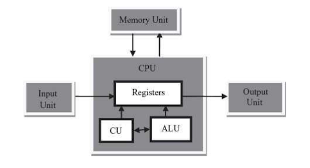
Two registers, the memory address register and the memory data register, act as an interface between the CPU and memory. The memory data register is called the memory buffer register by some computer manufacturers.
Figure 7.4 is a simplified representation of the relationship between the MAR, the MDR, and memory. Each cell in the memory unit holds 1 bit of data. The cells in Figure 7.4 are organized in rows. Each row consists of a group of one or more bytes. Each group represents the data cells for one or more consecutive memory addresses, shown in the figure as addresses 000, 001, . . . , 2^{n − 1}.
In modern computers, it is common to address 8 bytes at a time to speed up memory access between the CPU and memory. The CPU can still isolate individual bytes from the group of eight for its use, however.
The memory address register holds the address in the memory that is to be ‘‘opened’’ for data. The MAR is connected to a decoder that interprets the address and activates a single address line into the memory. There is a separate address line for each group of cells in the memory; thus, if there are n bits of addressing, there will be 2^n address lines.

The memory data register is designed such that it is effectively connected to every cell in the memory unit. Each bit of the MDR is connected in a column to the corresponding bit of every location in memory. However, the addressing method assures that only a single row of cells is activated at any given time. Thus, only one memory location is addressed at any one time. A specific example of this is shown in Figure 7.5. (Note that in the drawing msb stands for most significant bit and lsb for least significant bit.)

Comments
Post a Comment